Flexible future for electronics
Ben Smye, Head of Growth at materials resource and search engine Matmatch, explores how a new paradigm shift in stretchable electronics could herald further innovation.

Ben Smye, Head of Growth at materials resource and search engine Matmatch, explores how a new paradigm shift in stretchable electronics could herald further innovation.
Are sustainable, wearable electronics too good to be true?
An ultra-thin and fully transparent material, which is said to have one of the highest mobilities of any wide bandgap, positively charged semiconductor, is under development at RMIT University, Australia, for integration into flexible displays and smart lenses.

A technical lecture from the South Wales Materials Society
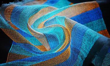
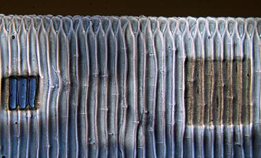
What is said to be the ‘largest’ glowing, flexible textile display is being weaved together using conductive polymer strands and luminescent fibres, allowing wearers to read messages or instructions and communicate through their sleeve. Reaching 6m long, the flexible textile display can be folded, bent and withstand 100 cycles in a washing machine.
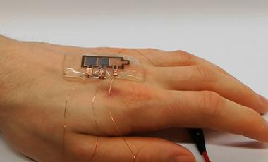
Bridging the gap between machines and the human body, a soft electronic ‘living’ material may facilitate medical diagnostics and treatments in real-time through its inherent controlled release of drugs and sensing capacity.
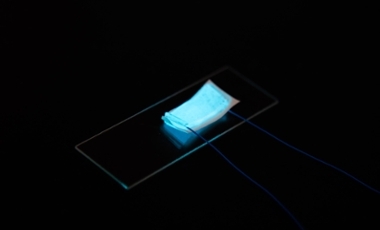
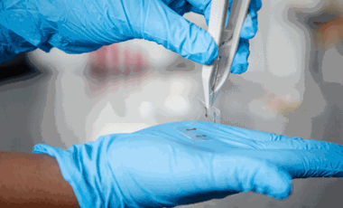
A stretchable material that can repair itself also illuminates visibly at low voltages. Shardell Joseph finds out how.
A conductive copper-nickel ink for printed electronics offers improved resistance to oxidation, say scientists at the National Institute for Materials Science (NIMS) in Japan.
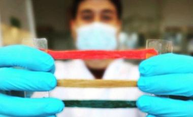
A team of researchers at the Swiss Federal Laboratories for Materials Science and Technology (Empa) has developed a flexible, shellac-based ink for printed circuits that they claim is metal-free, non-toxic and disposable.

Consortium includes Google, Microsoft and World Economic Forum.
This could lead to a variety of customised electronic devices using only a single element.
High-heat conductivity magnesium alloys that can reduce the weight of radiators and heat removal systems in electric vehicles and consumer electronics are being put forward by scientists in Russia.
A technical lecture from the South Wales Materials Society
Exploring EDX/EDS, EBSD and ion beam techniques for advanced materials characterisation
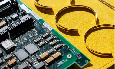
The Royal Mint’s new factory in South Wales will extract gold from e-waste and reduce reliance on virgin materials through mining.
Scientists at the University of Manchester, UK, are developing a world-first transmission electron microscope (TEM) that integrates artificial intelligence and automated workflows.
Findings come from joint study between University of Nottingham and NPL.
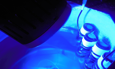
A novel method using blue LEDs could help create useful chemical subunit and eliminate the need for precious metals in the production of pharmaceuticals and electronics, researchers from the Hokkaido University, Japan, claim.
Dr Michael Ford MIMMM at Haseltine Lake Kempner explores a patent relating to hexagonal boron nitride on silicon-based substrates.

A gelatine and glucose-based film is said to be capable of repeatedly fixing cracks in its own structure within minutes, while preserving the functionality of the electronics in which it operates.