Nanoscale elementary semiconductors with tuneable electronic properties
This could lead to a variety of customised electronic devices using only a single element.
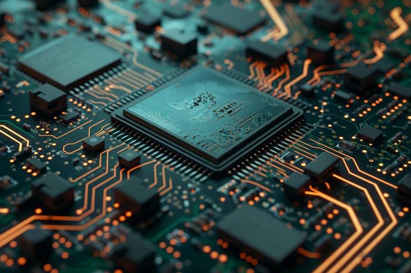
A computer circuit board featuring a central processing unit
© Sach336699 / ShutterstockThe inter-university group reports moulding a semiconductor with flexible bonds into various structures using nano-containers, without altering its composition.
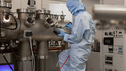
The group from the University of Nottingham, the EPSRC SuperSTEM facility, Ulm University in Germany, and BNNT LLC in the USA imaged new forms of selenium using transmission electron microscopy, employing nanotubes as tiny test tubes.
Semiconductors have a band gap, which determines how they conduct electric current. This is typically engineered for specific applications by breaking chemical bonds or introducing additional elements into the material, but the team says this can be complex and energy-intensive.
Selenium can exist as nanowires, with its structure and bonding varying by diameter. Below a certain size, the bonding between selenium atoms changes, increasing bond angles. This causes straightening of the initially helical structure, ultimately constricting it into atomically thin wires.
Dr Will Cull from the University of Nottingham says, ‘To our astonishment, we observed that the nano test tube became thinner as we imaged it!...This serendipitous discovery allowed us to establish mechanisms for the transformation of one type of nanowire to another, which have implications for their electronic properties, with near-atomic precision.’