Seeing through semiconducting material for transparent electronics
An ultra-thin and fully transparent material, which is said to have one of the highest mobilities of any wide bandgap, positively charged semiconductor, is under development at RMIT University, Australia, for integration into flexible displays and smart lenses.
‘The material can effectively conduct electricity and can be used in practical electronic devices. [It] has a wide electronic bandgap, this means that it is completely transparent to the human eye,’ says Dr Torben Daeneke, Professor and Team Leader at the University.
He adds, ‘Our beta-tellurite (TeO₂) is the first p-type (positively charged electrons) oxide that has a comparable carrier mobility to n-type (negatively charged electrons) oxides. Since both types of semiconductors are often required when making devices, the discovery of a high mobility oxide closes a crucial gap in the available materials spectrum.’
Daeneke explains that oxide semiconductors can either come as p-type or n-type semiconductors. P-type semiconductors use electron-vacancies (holes) as their principal charge carriers, while n-type oxides use electrons. N-type oxides are very well developed, however, p-type oxides tend to fall short in performance.
‘This is a significant finding since oxide electronics have been intensely investigated for decades,’ Daeneke says, ‘but the lack of a high mobility p-type oxide was hampering progress. The main reason for the high mobility is that tellurium is in the same group of the periodic table as oxygen. This had profound effects on the bonds within the material which ultimately resulted in the high performance.’
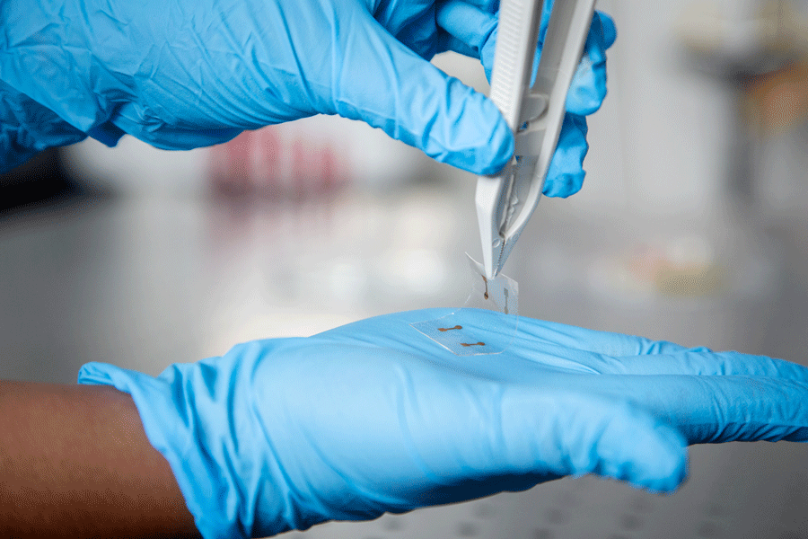
He notes that the oxide-based material is 1.5nm thick. ‘We essentially designed a low melting tellurium-selenium alloy that is allowed to oxidise in air. The alloy melts at about 200°C and can be dragged across a surface using a glass tip. As the alloy droplet is moved over the surface, the TeO₂ nanosheets are deposited in its path. The method is essentially similar to pen writing. This process should be conducted in a proper lab environment though, since selenium is quite toxic. We are working to replace selenium as we speak.’
The team suggests that because the material is ultra-thin, it is flexible. It also has less stringent purity requirements, low cost, easy deposition, and since it is an oxide, it is also stable in air.
They also claim that it has one of the highest mobilities of any wide bandgap p-type semiconductor, and is about ten to a hundred times faster at transporting signals than metal oxide semiconductors. ‘This has profound effects on the quality of electronics that may be made using these nanosheets,’ says Daeneke, who notes that it is one of the first oxide materials to come close to silicon in performance.
‘As such, this work enables the design of new electronic devices that are flexible or transparent while not having to compromise on computing speed.’
The team is now looking to develop this material further. ‘On one side we are exploring the physical properties of beta TeO₂ in our labs and are looking at some exciting new phenomena that arise in this material,’ Daeneke says.
‘Simultaneously, we are looking at better ways of making these nanosheets in order to incorporate them at a larger scale into devices. We are also looking to partner up with industry to develop this technology further and ultimately create some of these new types of electronics.’