High-temperature superconductors for MRI applications developed
A group of scientists led from Nagoya University, Japan, developed an inexpensive, scalable way to produce high-temperature superconductors using ‘grain boundary engineering’ techniques.
The new method could help develop stronger, inexpensive, and high-operating temperature superconductors with impactful technological applications.
Key to the dissipation-free conduction of currents in superconductors in the presence of a magnetic field is a property called ‘pinning potential’. Pinning describes how defects in the superconducting matrix pin vortices against the Lorentz force. Controlling the micro-structure of the material allows for careful introduction of defects into the material to form artificial pinning centres (APCs), which can then improve its properties. The most common approach to introducing such defects into superconductors is ‘ion irradiation’. However, ion irradiation is both complicated and expensive.
In their study published in NPG Asia Materials, Professor Kazumasa Iida and his research team successfully grew a thin film superconductor that has a surprisingly high pinning efficiency without APCs. ‘Crystalline materials are made up of different regions with different crystalline orientations called 'grains.' When the angle between the boundaries of different grains in the material are less than their critical angle, θc, we call it a 'low-angle grain boundary (LAGB).' LAGBs contribute to magnetic flux pinning, which enhances the properties of the superconductor,’ explains Dr. Iida.
Iron (Fe)-based superconductors (FBS) are considered to be the next-generation superconductor technology. In their study, Professor Iida and team grew an FBS called ‘potassium (K)-doped BaFe2As2 (Ba122)’ using a technique called ‘molecular beam epitaxy,’ in which the superconductor is grown on a substrate. ‘The difficulties involved in controlling volatile potassium made the realization of epitaxial K-doped Ba122 challenging, but we succeeded in growing the thin films on fluoride substrates,’ says Dr. Iida.
The team then characterised the FBS using transmission electron microscopy and found that the film was composed of columnar grains approximately 30-60 nm wide. These grains were rotated around the crystallographic principle axes by angles well within θc for K-doped Ba122 and formed LAGB networks.
The researchers then performed measurements of the thin film's electrical resistivity and magnetic properties. They observed that the thin films had a surprisingly high critical current (the maximum current in a superconductor above which it transitions to a dissipation state). The LAGB networks further ensured a strong pinning efficiency in the material. ‘The in-field properties obtained in our study are comparable to that of ion-irradiated K-doped Ba122. Moreover, grain boundary engineering is a simple technique and can be scaled up for industrial applications,’ comments Iida.
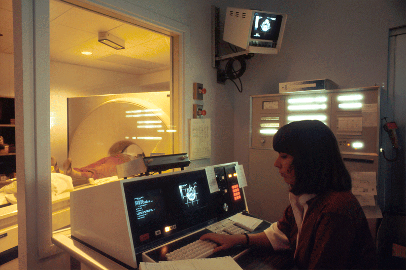
The findings of this study could accelerate the development of strong magnets using superconductors, leading to advances in magnetic resonance imaging (MRI). The widespread application of MRI is currently limited by the high investment and operational cost of the MRI machines due to the cooling costs of the superconductors within. But with simple and inexpensive techniques such as grain boundary engineering for fabricating superconductors, MRIs could become more accessible to patients, improving our quality of life.