Mass production of metalenses for visible wavelengths
The first successful mass-production of metalenses for visible light is being claimed by South Korean researchers.
The production requires sub-100nm resolution nanofabrication, claim the group from Pohang University of Science and Techology (POSTECH).
To overcome the limitations of the fabrication process they have combined two techniques used in semiconductor and display manufacturing – photolithography uses light to pattern a substrate, while nanoimprint lithography involves a stamp with nano-sized patterns to print them onto a substrate.
They explain how conventional methods like electron-beam lithography (EBL) have a high enough resolution to use in the visible wavelength, but it is expensive, time-consuming and can only produce metasurfaces that span small areas.
Meanwhile, there are also critical problems in the refractive index of the resin in nanoimprint lithography – only a few materials with relatively low refractive indices can be used.
Professor Junsuk Rho, the lead researcher, says 'To overcome these limitations, several works recently used photolithography, including deep-ultra-violet (DUV) photolithography; however, material, resolution and manufacturing cost limitations still remain.'
So far, metasurfaces that operate in the near-infrared have been demonstrated at the wafer scale using a krypton fluoride laser (248nm) DUV photolithography.
Rho says, 'We addressed the critical bottlenecks of commercialisation through the combination of argon fluoride (ArF, 193nm) DUV photolithography, nanoimprinting, and a new high-index material consisting of a hybrid, atomic-layer, polymer resin.
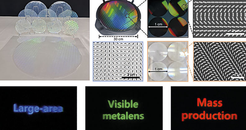
'Photolithography has the advantage of being able to precisely create master moulds on a wafer scale, while nanoimprint has the advantage of being a very fast and cost-effective patterning method. By combining the advantages of nanoimprint and photolithography, we achieve superior performance in terms of time taken, throughput and cost, owing to the wafer-scale nanoimprinting and reusability of the wafer-scale mould.' ArF immersion lithography was used to fabricate a 30.48cm master mould, which was then replicated using a double-polydimethylsiloxane layer.
Rho says, 'Once this master stamp is imprinted and thinly coated with a high-index film, we can produce hundreds of centimetre-scale, high-efficiency metalenses.'
They use atomic layer deposition (ALD) to coat a thin layer of high-index titanium dioxide (TiO2) to enhance the birefringence of the meta-atom (Δn = 0.22, effective index is about 2.1), resulting in a 10-90% increase in the conversion efficiency. The TiO2 film is around 20nm thick, resulting from the elaborate modal analysis, and the hybrid meta-atom strongly confines the light.
Previous studies using TiO2 in the visible wavelength required thick ALD deposition to achieve a height of several hundred nanometres. In comparison, this method is reported to achieve high efficiency with a very thin film, allowing implementation of an ideal lens.
Key to this process is that the complementary metal-oxide semiconductor (CMOS) is compatible with wafer-scale fabrication and it is possible to replicate on various substrates using imprinting techniques. Rho shares that the master mould and stamp can be used repeatedly for over 20 cycles.
The team has obtained over 650 metalenses with a diameter of 1cm in about 15 minutes using this process. With a reusable mould, and by creating multiple master stamps and performing the process simultaneously, production can increase further.
Additionally, 'we can modulate the optical properties of hybrid materials by simply varying the high-index material and polymer,' explains Rho. Functional nanoparticles can be merged into the imprinted resin, and the atomic-layer thin-film can be replaced with other functional films. Thus, the target wavelength of the metasurface can be 'easily tuned by coating different materials with a high refractive index at the target wavelength'.
Remaining issues to overcome are: reliance on EBL to create the initial 4cm-sized reticle, the challenges of creating larger metalenses due to CAD file sizes, and developing high-performance materials that can achieve various functionalities at numerous wavelengths.