Photovoltaics come indoors to power wireless smart devices
The development of lead-free perovskite-inspired materials (PIMs) that convert ambient indoor light into electricity could power wireless smart devices in the future, following findings of a joint international research project.
In what the scientists claim is the first study on PIM indoor photovoltaics, they suggest this will reduce energy consumption as it allows for some of the energy used to illuminate indoor environments to be harvested and recycled. An additional benefit is that it would reduce the consumption of batteries needed to power electronic devices.
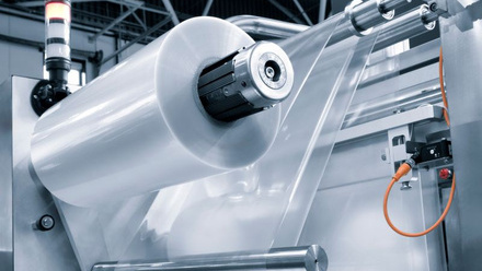
The team from the University of Cambridge, UK, Imperial College London, UK, and Soochow University, China, has developed two materials – caesium antimony chloride-iodide (Cs3Sb2ClxI9-x) and bismuth oxyiodide (BiOI). Although these PIMs are not as efficient at absorbing sunlight, they have been found to be effective at absorbing indoor light. They are being applied in solar cells to demonstrate efficiencies (~5%) comparable to the current commercial technology for indoor photovoltaics based on hydrogenated amorphous silicon.
Bismuth replicates many of the electronic features of lead but produces non-toxic and safe materials, says the team. Crucially, the researchers have demonstrated that the power provided by these materials under indoor illumination is already sufficient to operate electronic circuits, with an absorption profile that closely matches the light spectrum of common indoor bulbs.
The materials do not, however, share the crystal structure of, and are not classed as, perovskites. Instead, they have a similar layered crystal structure to graphite.
The Cs3Sb2ClxI9-x is developed using a process that resembles watercolour painting. A solution of an organic solvent and halide salts of caesium and antimony is spread over a substrate (e.g. made of glass, but also plastics). While the solvent evaporates, the halide salts self-assemble in a way that leads to a perovskite-derivative structure, thereby leaving the substrate with a coating of Cs3Sb2ClxI9-x.
BiOI, meanwhile, is grown using chemical vapour deposition. The reactants, bismuth iodide and oxygen gas, are introduced to the reactor in the vapour phase. Bismuth iodide absorbs on the substrate and reacts with oxygen to nucleate and grow grains of bismuth oxyiodide, which appear as micron-sized flakes connected together to form a thin film.
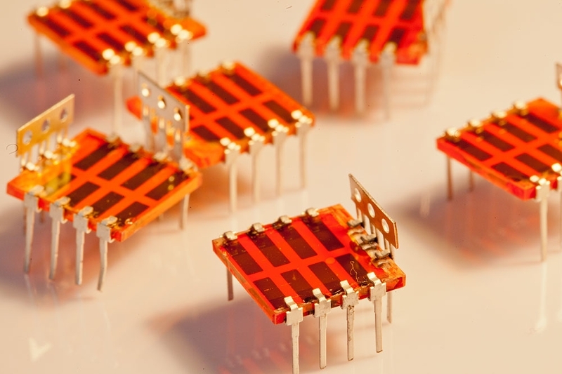
To make a functioning solar cell, the bismuth oxyiodide is, for example, sandwiched between semiconductors that selectively extract charge. These, in turn, are encased between two electrodes, one metal and the other transparent, so that light can be absorbed from LED bulbs or fluorescent tubes.
After absorption, a built-in electric field forces the electron in the conduction band and the hole in the valence band to reach opposite electrodes. This achieves ‘clean electricity’ from light with no mechanical moving parts and no CO2 emitted.
As demand has grown for lead-free and stable alternatives that can replicate the electronic properties of lead-halide perovskites, researchers have turned to PIMs to meet demand.
“We investigated them because of their potential to replicate the key features of the lead-halide perovskite electronic structure that would enable them to mimic the ability to achieve efficient performance despite many imperfections being present in the materials,” says Dr Robert Hoye FIMMM at Imperial College London.
“We call this ‘defect tolerance’ [which] enables efficient devices made at low-cost. [This] is the holy grail for researchers working on next-generation optoelectronics.”
The team adds that both materials are stable for several months when they are kept in an inert environment. This is important because it simulates the conditions the materials will experience in commercial devices that are fully packaged.
The next steps are to achieve higher efficiencies for the specific PIMs. “Additionally, we calculated the ultimate indoor photovoltaic efficiency of a larger set of PIMs,” explains Professor Vincenzo Pecunia of Soochow University. “In particular, we showed that PIMs have the potential to reach indoor photovoltaic efficiencies between 40-60%, which would be a tremendous improvement over current...technologies.”
Professor Judith Driscoll FIMMM, from the University of Cambridge, adds, “The Internet of Things (IoT) is critical for many areas, such as improved healthcare, energy conservation, transportation or control of smart buildings. New generations of wireless-connected IoT devices [that] function with low-power electronics [are] ideally suited to operate with energy-scavenging devices.”
The team notes that even if a continuous supply of power is required, PIM-based indoor photovoltaics could be combined with batteries to recharge them wirelessly. This would then allow the operational lifetime of the electronic device to be extended to the actual lifetime of the hardware itself.