Zinc-based electronics on biodegradable surfaces
The circuit board design on paper and bioplastics is reportedly almost entirely biodegradable.
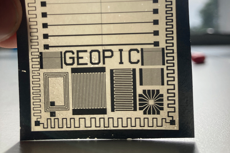
The zinc circuit board
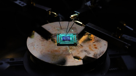
© Glasgow UniversityResearchers at the University of Glasgow, UK, say 99% of the circuit materials can be disposed of safely with ordinary soil composting, or by dissolution in widely available chemicals like vinegar. The remaining 1% that cannot be disposed in this way is largely due to the light-emitting diodes (LEDs).
Conventional circuit boards are made from difficult or costly-to-recycle materials. The team is tackling the problem by developing a ‘growth-and-transfer additive manufacturing process’, which generates conductive metal tracks on biodegradable surfaces.
Unlike conventional circuit boards, which use copper to conduct electricity, the team use zinc instead to create metal traces just 5µm wide. The process works by electroplating conductive bulk zinc onto a temporary aluminium carrier. The tracks are then transferred to a biodegradable base.
Dr Jonathon Harwell at the university explains, 'The photoresist then acts as a stencil…letting us make any design we want. This leaves us with our desired track pattern floating on top of the aluminium carrier, and we designed the electroplating process to ensure that these tracks are only very weakly adhered to the aluminium – just enough to keep them in place but weak enough to be easily separated (this was the hardest part of the process).'
Harwell continues, 'Finally, we transfer to the new material (e.g. a bioplastic) by melting it and pouring it over the tracks. Once it has solidified, then we can simply peel it off the aluminium substrate, and it takes the patterned tracks with it… we use chitosan…as a glue to bond the tracks to the paper.'
Harwell adds, 'We made samples on other biopolymers such as chitosan, non-degradable materials…and we even made some working samples out of glucose, or even chocolate. The chocolate [printed circuit board] PCB is completely useless'. But they made it to illustrate the flexibility of the application.
The difficulty in making complex metal patterns on biodegradable materials is usually down to the harsh conditions needed for patterning that tend to destroy or warp the materials. Here, the process is separated to make the patterns on a durable and reusable carrier substrate and then they are transferred onto the biodegradable material. This means the fragile biodegradable materials never come into contact with the harsh patterning conditions.
The resulting circuits reportedly perform comparably to traditional boards, and the team has tested them in multiple devices, including tactile sensors, LED counters and temperature sensors.
Zinc has about a third of the conductivity of copper, but still 'more than sufficient' for most applications, Harwell suggests. The team reports poor performance under high-frequency applications in the MHz-GHz regime because biodegradable materials contain trapped water, but they are not targeting such devices.
Additionally, the tracks are said to be durable and scratch-resistant because they are embedded into the final material with great adhesion while being flush to the substrate surface. The first samples made, almost two years ago, still work with 'no drop in conductivity' and are 'remarkably stable' in air conditions, says Harwell.
'However, under warm, wet conditions they degrade rapidly as the paper biodegrades and the zinc dissolves into zinc oxides' as designed. They can enhance sample stability in water by adding coatings such as cellulose acetate, but this means a trade-off of slower biodegradation.
A Life Cycle Assessment reveals that the biodegradable PCBs could enable a 79% reduction in global warming potential and a 90% reduction in resource depletion.
Harwell claims, 'It’s really cheap and can be done with off-the-shelf chemicals and consumer-grade electronics. You can replicate the entire process for small PCBs with 0.2mm resolution tracks with less than £1,000 of equipment and starting chemicals.' However, patterning larger areas with finer resolutions will require more 'involved set-ups'.
Harwell adds, 'Our work was inspired by the progress in printed electronics, but we aimed to circumvent the issues with making conductive inks using electroplating, and the real breakthrough came when we found ways to control the adhesion of the plated metal to carrier substrate', essential in getting an effective transfer.
'We are focusing on the ‘ultra-disposable’ end of applications such as smart labelling or throwaway medical devices.'