Multi-purpose paper semiconductor takes shape
A nanocellulose paper semiconductor that is tuneable to flexible devices is the product of a Japanese research collaboration.
The team, from Osaka University, the University of Tokyo, Kyushu University and Okayama University, has made a semiconductor with the potential for ‘nano-micro-macro trans-scale designability of 3D structures’.
Cellulose nanofibres, or nanocellulose, from bleached softwood, or other wood pulp, are turned into flexible nanopaper sheets by mechanical nanofibrillation.
While nanopaper can be made conductive through heating, it can disturb the nanostructure. The researchers use an iodine treatment to protect the nanostructure, as well as spatially controlled drying to prevent the pyrolysis altering the design. Specific temperatures dictate the conductivity.
The researchers say that their semiconductor has tuneable electrical resistivities in the 10¹²−10−²Ωcm range (conductivities in the 10−¹²−10²S cm−¹ range), which they believe largely exceeds that attained by other reported semiconducting nanomaterials.
Lead researcher Hirotaka Koga explains that pyrolysis removes carbon and hydrogen as a hydrocarbon gas, but the iodine-mediated pyrolysis suppresses carbon removal by forming hydrogen iodide.
Koga says, ‘When the nanocellulose/water dispersion was dried, a densely packed nanostructure was obtained due to agglomeration because of the capillary force generated by the high surface tension of water. Solvent exchange with tert-butyl alcohol with a low surface tension and subsequent freeze-drying afforded porous nanofibre-network structures with pore sizes of less than 100nm. Freeze-drying of concentrated nanocellulose in water dispersion formed honeycomb-shaped microstructures with pore sizes of several micrometres, which are consistent with the shape of an ice crystal.’
The team has used origami and kirigami paper cutting techniques to showcase the semiconductor’s flexibility.
Koga continues, ‘The nanocellulose paper semiconductor has many advantages over conventional semiconducting nanomaterials, such as lightweight (bulk density less than
0.3g/cm3) and sustainability, as well as nano−micro−macro trans-scale designability of the 3D structures and wide tunability of the electrical properties.’
Heating the semiconductor once enables it to retain its conductivity, which can be controlled through the pyrolysis.
‘We found that both the nano−micro−macro trans-scale designability of 3D structures (in the nanometre−centimetre range in terms of pore size, surface structure, and macroscopic morphology), and wide tunability of electrical resistivity, are notable features of the nanocellulose paper semiconductor that are better than those of previously reported 3D semiconductor structures,’ Koga shares.
Potential applications are sensing, energy storage and energy-generation due to a high-surface-area nanomorphology of up to 720m2g-1.
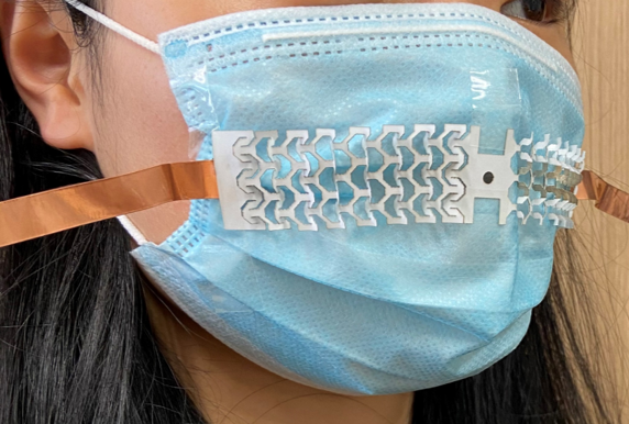
The semiconductor has been incorporated into a facemask by preparing it at a carbonisation temperature of 600°C, (a resistivity of the order of 104Ωcm), creating a 5mm diameter circle and pasting it onto a stretchable paper substrate.
In a biofuel cell, it was prepared at 1,100°C, at a size of 1×1cm, with tailored nanoscale pores and quasi-conductor properties with an electrical resistivity of 4.5×10⁻²Ωcm. The semiconductor is said to have 14 times higher power density than a commercial graphite electrode (~10μW cm2), with high electrical conductivity and efficient enzyme-immobilisation properties.