Is graphene the answer to the semiconductor shortage?
A new initiative has been set up by European research initiative Graphene Flagship to integrate graphene and layered materials into semiconductor platforms.
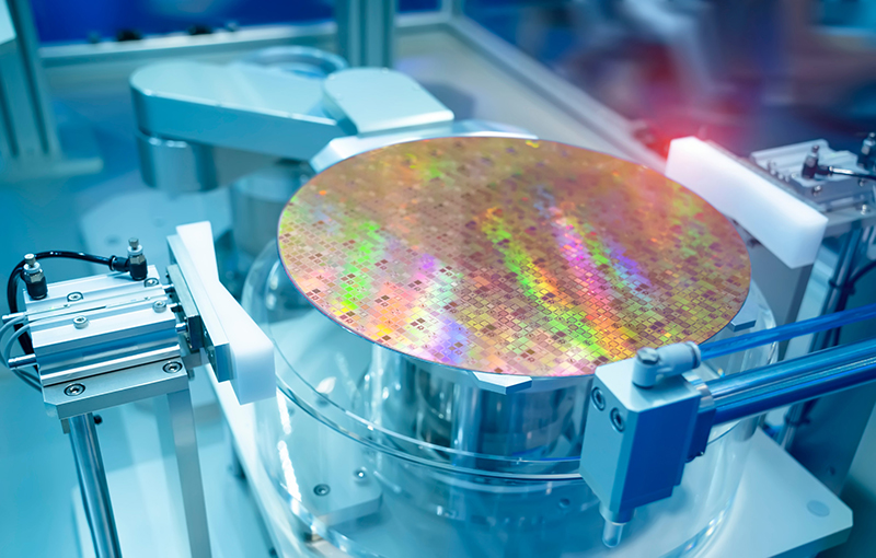
The 2D Experimental Pilot line (2D-EPL) is said to be the first graphene foundry to pioneer graphene-integrated wafers for new prototype electronics, photonic devices and sensors.
This will involve producing a multipurpose graphene wafer (MPW) — or 'planarization based generic platform' — that will eventually be mass-produced for a variety of applications and sectors. Measuring 200mm in diameter, the MPW is made from polycrystalline chemical vapour deposition (CVD) graphene and combines existing technologies by several 2D-EDL partners.
The initiative will also offer prototyping services to companies, research centres and academics, so they can develop and test their technologies based on 2D materials.
The team believes such 2D materials could help alleviate the shortage of semiconductors.