How materials for solar photovoltaics will combat climate change
Professor Stuart Irvine discusses the potential for increasing the implementation of solar PV electricity and the challenges for materials development.
Over the past 10 years there has been a dramatic increase in global energy supplies from renewable energy, particularly from wind and solar. Back in 2012 the global installed capacity of solar photovoltaic (PV) panels was around 100 GW, last year this had increased to a cumulative capacity of over 1 TW. During this time the efficiency of PV panels has increased from around 16% to more than 20% and the price has decreased to make it one of the cheapest sources of electricity. However, the backdrop is the climate crisis where time is running out on reducing our carbon emissions and containing global temperature increases. Over the same period the consumption of fossil fuels for all types of energy generation has actually increased from around 120,000 TWh to over 130,000 TWh. To reduce our emission from fossil fuels we will need to accelerate the introduction of all forms of low carbon energy. In this article I will look at the potential for increasing the implementation of solar PV electricity and the challenges for materials development.
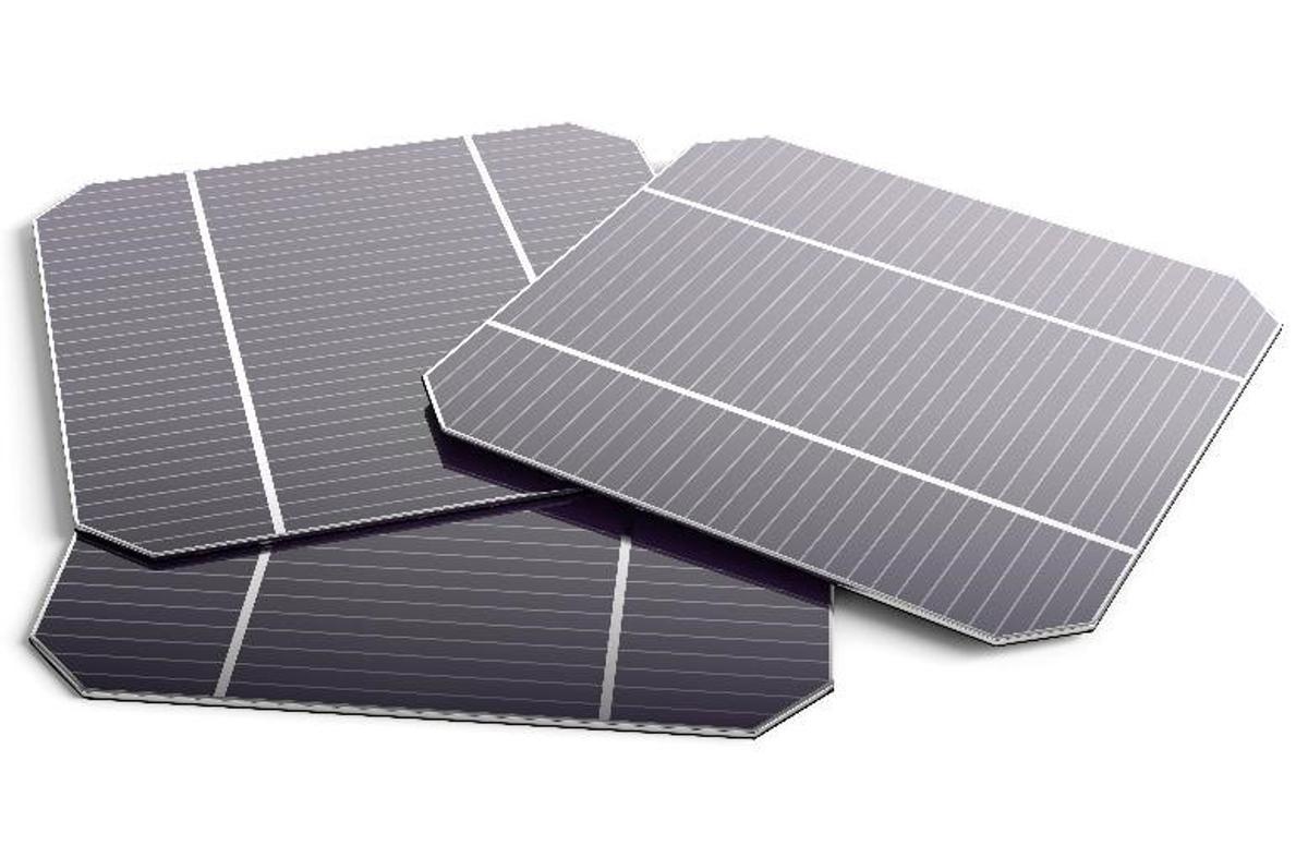
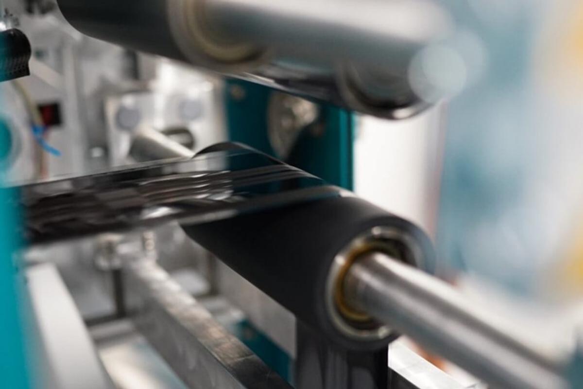
Over 90% of global production of PV panels is based on silicon with the remaining production using thin film cadmium telluride or copper indium gallium selenide (CIGS). Ten years ago silicon production was based on multi-crystalline silicon (Multi-Si) which is cheaper to produce but less efficient than mono-crystalline silicon (Mono-Si). Production is now dominated by Mono-Si where cost has come down through increased production volume, production of larger diameter crystals and use of thinner wafers in the production of solar cells. The benefit to this switch is an increase in efficiency of the conversion of solar energy into electrical energy. Efficiency not only increases the amount of solar electricity generated per square metre but also helps to reduce the cost of solar electricity. While production of the materials has been undergoing a revolution there has also been big changes in the design of silicon cells to give a further boost in efficiency. Production is now dominated by the Passivated Emitter and Rear Contact (PERC) cells. Below is an image of silicon solar cells that can be connected in a string and laminated with glass for manufacture of the familiar silicon PV modules. The PERC device structure reduces the recombination of photo-generated charge at the back surface, allowing more charge to reach the top surface p-n junction. Other more advanced device structures could push the cell conversion efficiency even higher but there is a physical limitation to the efficiency of a single junction solar cell, called the Shockley-Quiesser limit which is around 30%, depending on the absorber material.
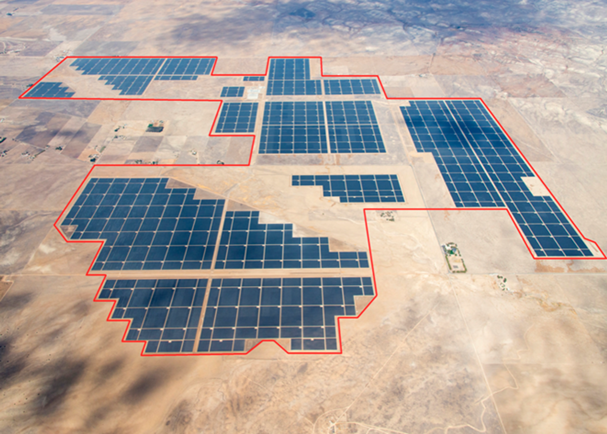
Although silicon dominates global production, thin film PV has also expanded production. So, what is the motivation for these alternative materials as thin film coatings? Thin film PV is also constrained by the same Shockley-Quiesser limit on single junction efficiency. However, production costs are lower due to lower temperatures for thin film materials synthesis, typically less than 600 °C, hence lower energy costs in processing the materials. So why isn’t the PV market dominated by thin film PV? For the past 20 years thin film PV has been playing catch-up in both production scale and the efficiency of the panels. One company, First Solar Inc. have dominated the thin film PV market for much of this time and shown that large scale production is possible using cadmium telluride thin film PV. First Solar Inc. is the only non-silicon PV panel producer in the top 10 of suppliers with current annual shipment around 8 GW and predicted to increase to 25 GW in 2025. These panels are mostly used for large utility scale PV and an example is shown below. The current panel efficiency is 19%, slightly lower than that for silicon. Intensive research in complex materials issues including polycrystalline microstructure, surface passivation and electrical doping could lead to a predicted cell efficiency of 25%. The electrical doping of the p-type cadmium telluride has limited cell voltage to less than 900 mV whereas a cell voltage of 1.2 V should be possible. Copper doping is used in the current panel design but a switch to arsenic doping could improve the electrical doping by a factor of 100. However, performance is not straightforward in complex semiconductor materials and a better understanding of the electrical behaviour of doping in these materials is needed before the anticipated improvement in efficiency will be realised.
The practical efficiency of current designs of PV panels, silicon and thin film, is limited to around 25%, partly due to the Shockley-Quiesser limit and practical materials limitations. However, the story doesn’t stop there. The Shockley-Quiesser limit can be exceeded with multi-junction cells where each junction is designed to capture a different part of the solar spectrum. Intensive research into 2-junction cells on silicon has captured much interest from industry with the prospect of over 30% efficient panels. An attractive front runner for this development combines perovskite thin film solar cells with well-established silicon solar cells. Perovskites are a class of materials with the perovskite structure ABX3 where 'A' is methyl ammonium, 'B' is a metal such as lead or tin, and 'C' is a halide. The manufacturing process can be scaled using printing processes. The most efficient laboratory cells have reached a record of 25.7% which has more than doubled in 10 years. The composition can be readily adjusted to change the bandgap which can be tuned to provide an efficient top cell for silicon. Oxford Solar are leaders in developing this technology with their research centre in Oxford and a pilot production facility in Germany. They have recently achieved a new world record for a tandem device on a full size silicon wafer of 28.6%. This exceeds expectations for a single junction silicon cell and paves the way for high efficiency PV panel manufacture, exceeding 30%, in the future.
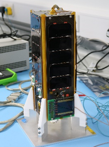
Terrestrial solar power is limited by daylight hours and suffers losses due to atmospheric absorption and cloud cover. This can reduce the energy generated to less than 20% of the maximum expected from the rated power, which assumes constant solar irradiation. A lot of factors will determine the predicted solar energy generation over an annual cycle, including latitude, weather, orientation of panels and shading. A new approach, Space Based Solar Power (SBSP) has the potential to generate electricity close to the power rating of the solar cells for most of the day. Large PV arrays in Earth orbit will continuously beam the energy to ground based stations using microwaves. Space has none of the environmental limitations of the Earth surface and by careful selection of orbit can minimise the time in Earth eclipse. The cost of launch must be minimised by using very lightweight PV solar arrays, where thin film PV materials are bonded to radiation hard ultra-thin glass. Satellites are now almost entirely powered by very efficient multi-junction indium gallium phosphide (InGaP) and indium gallium arsenide (InGaAs) solar cells grown onto germanium or gallium arsenide substrates. Lift-off techniques can be used to separate the multi-layer thin film PV structure from the substrates that are then re-used, saving cost and weight. An alternative approach is being pioneered at Swansea University where thin film cadmium telluride is deposited directly onto the ultra-thin glass producing a robust and very light weight structure. A successful flight test of these solar cells is now in its 6th year on the AlSat-1N mission and is still sending back data. Much has been learned from the data transmitted back to the base station and a further flight test is planned for next year. This approach is lower cost than the InGaP/InGaAs multi-junction solar cells but currently achieves much lower efficiency for solar conversion. In the future, multi junction thin film CdSeTe/CdZnTe solar cells could significantly boost this efficiency while retaining the low cost and superb radiation hardness.
The expansion of solar power is expected to increase rapidly over the next few decades, will become more efficient in solar energy conversion and lower the price of electricity. Materials developments will be central to this expansion and help a continual improvement in solar PV technology. We will see more integration of solar PV into everyday life from different forms of building integrated PV to a vast array of monitoring devices, referred to as the 'internet of things'. All these developments will be helping to reduce the impact of climate change and providing a more sustainable future.
Authors