Fishing for atoms - probing behaviour at solid-liquid interfaces
Scientists at the University of Manchester, UK, on a new approach to probe atomic behaviour at solid-liquid interfaces.
This article was compiled by Professor Sarah Haigh, Professor Roman Gorbachev, Dr Nick Clark and Matt Lindley at the University of Manchester, UK.
Probing the behaviour of atoms or ions at solid-liquid interfaces is key to understanding a wide range of material science processes, including heterogenous nucleation and growth, electrochemical reactions and many catalytic reactions.
Over the last 25 years, aberration corrected transmission electron microscopy (TEM) has become a key characterisation tool to reveal surfaces and interfaces, due to its ability to provide atomic resolution imaging of local structural features coupled with complementary elemental analysis.
The TEM forms images by detecting changes induced in the electron beam as it passes through a sample. The ability to reveal atomic structure even at the level of single atomic species is due to the electron beam’s strong interaction with matter.
Yet this same strong interaction also produces a stringent requirement for the maximum allowable sample thickness to ensure the electron beam can pass through – a thickness of less than 10nm is often recommended for high-quality atomic resolution imaging (equivalent to 30 atomic planes in graphite). In practice, samples are often slightly thicker than this.
Obtaining an ultra-thin specimen while remaining representative of the material of interest is the first big challenge of performing TEM analysis.
The second key challenge is the TEM’s high vacuum environment, which is problematic when analysing solid surfaces that operate in liquid or gaseous conditions (solid-gas and solid-liquid interfaces).
The limitations of a vacuum environment for analysing materials was recognised as far back as the 1940s, including by Ernst Ruska, one of the original inventors of the electron microscope. However, scientific progress in this area was limited until the development of the environmental transmission electron microscope (E-TEM), pioneered by Pratibha Gai and Ed Boyes, now at the University of York, UK. E-TEMs use differential pumping to enable the sample to be imaged surrounded by a low pressure of gas (typically 5m bar), while a vacuum is maintained within the rest of the microscope and importantly around the electron source.
The last decade has seen an increasing body of scientific work, largely focused on nanoparticle catalysts, demonstrating that the surface structure of metallic and metal oxide nanoparticles depends critically on the local gaseous environment.
For example, seminal work by Seiji Takeda and colleagues at Osaka University, Japan, used an aberration-corrected E-TEM to directly visualise the atomic surface reconstruction of ceria-supported gold nanoparticles, due to the presence of adsorbed carbon monoxide (CO).
However, E-TEMs are limited to relatively low gas pressure, or the gas thickness becomes too great and the imaging resolution is severely compromised. They are also not compatible with imaging liquid-phase specimens, unless the liquid has a high vapour pressure as is the case for ionic liquids.
These limitations have driven major developments in in situ environmental cell (E-cell) TEM holders, where the sample is physically separated from the TEM vacuum using two electron transparent and impermeable membranes.
These in situ gas- or liquid-cells enable exciting possibilities for TEM imaging of specimens in environments that mimic reaction conditions. By incorporating electrical feed-throughs and gas/liquid channels from outside the microscope, they can perform mixing of liquids and gases at pressures of up to four atmospheres, apply heating up to ~1,000°C, and enable biasing and electrochemical cycling of the sample.
The principal drawback is that commercial in situ gas- or liquid-cells generally employ silicon nitride for the membrane windows with the total window thickness often exceeding 80nm. These windows, combined with the thickness of the liquid or gaseous environment, puts a limit on the achievable spatial resolution and severely restricts the potential for atomic resolution imaging, especially for liquid cells. Thinner windows are insufficiently robust and tend to fracture before TEM imaging can be performed.
The first atomic resolution TEM imaging in the presence of a liquid was therefore achieved using a different approach. A group of researchers at the University of California, Berkeley, USA, showed that bringing two sheets of graphene together in the presence of the liquid sample caused blister pockets to form at the interface. Atomic resolution was achievable where the pockets had a suitably small liquid thickness, with the two graphene sheets acting as perfect barrier membranes because of the material’s low atomic number, high mechanical strength and flexibility, impermeability to water, and ultimate (single-atomic layer) thickness.
The material also has further benefits – its chemical inertness reduces the change of reaction with the specimen and the excellent conductivity enhances the ability to scavenge aggressive electron-beam-induced radical species.
This first graphene liquid cell caused enormous excitement in the community, but the following 12 years has seen a relatively small number of further scientific publications deploying them. This is most likely due to experimental challenges – although the approach sounds simple, it relies on the random formation of liquid pockets between two graphene sheets, and therefore samples often exhibit low yield and poor stability.
To better understand the synthesis challenge, it is instructive to consider trying to transport soup between two flat sheets of cling-film – the soup adopts a random morphology and has a strong tendency to leak out from the interfaces where the sheets form creases.
Spacer crystal
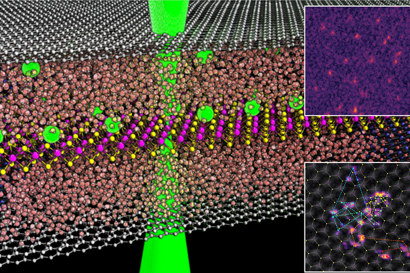
For the last five years, researchers at the University of Manchester, UK, have been developing an improved method for building graphene liquid cells shown in the image above. In our approach, a 2D ‘spacer’ crystal – graphene or hexagonal boron nitride – with a thickness of ~30nm is lithographically etched to define isolated wells for the liquid sample.
The bottom side is then sealed using graphene before filling the etched wells with liquid and sealing the top with graphene.
The dimensions of the liquid cell are precisely controllable by modifying the spacer crystal’s thickness and the dimensions of the lithographic etching.
The drawback is the additional experimental expertise required to first perform the lithographic etching and then manipulate the atomically thin sheets to combine the graphene windows and etched spacer crystal in the presence of liquid. Extending the soup analogy, we now have a sort of tiny tupperware or petri dish with the clingfilm suspended over the top and bottom. The result is an incredibly robust liquid cell and we have found that our samples still contained liquid two years after their original fabrication.
Recently, the fabrication of such cells has been extended to include two spacer crystals and hence two sets of liquid pockets. By introducing a sacrificial 2D separation membrane between the crystals (shown in image 3b on the previous page), this double-graphene-liquid-cell enables liquid-liquid mixing experiments to be performed by perforation of the separation membrane with the electron beam.
We have recently applied this approach to study the formation of calcium carbonate by mixing two aqueous solutions containing calcium chloride and sodium carbonate, respectively. Calcium carbonate synthesis is a complex process but its understanding is key for predicting the growth of many marine organisms, as well as to inform optimal synthesis routes for the material’s many commercial applications.
Our observations have revealed that the first sign of the reaction is the formation of a denser Ca-rich liquid phase, providing new experimental evidence for a non-classical synthesis route that has recently been theoretically proposed.
Dynamic behaviour
We find that this double-graphene liquid-cell design also provides a solution to the challenge of probing dynamic atomic behaviour on a surface in the presence of liquid. This had previously proved elusive even with earlier designs of graphene liquid cells, although Graham Hutchings group at Cardiff University, UK, has used ex situ vacuum TEM to show that the composition of the liquid environment during synthesis can change the distribution of gold on carbon from nanoclusters to single atoms.
The problem was that even though graphene is relatively robust to extended atomic resolution imaging, point defects and pores are inevitably created when the electron dose is sufficiently high to enable the specimen to be imaged with atomic resolution for extended periods. Our double-liquid-layer graphene cell design allows point defects to be created in the suspended central membrane without producing pores in the outer membranes, preventing loss of liquid from the cell.
To demonstrate the potential of this technology, we have investigated platinum adatoms on an atomic sheet molybdenum disulphide (MoS₂). The metal is deposited from an aqueous solution of platinum chloride in the graphene liquid cell.
The interaction of sparse metal dopants with the surfacesof 2D materials has attracted research interest for a diverse range of applications including heterogenous catalysis, lubrication, data storage and filtration. Adding platinum to MoS2 is known to enhance the material’s catalytic performance towards the hydrogen evolution reaction, compared to either component in isolation. However, previous ex situ TEM imaging has shown that the platinum is almost entirely associated with the presence of sulphur vacancies. Our atomic resolution graphene liquid cell experiments have found a platinum adatom distribution that more accurately reflects the behaviour predicted by density functional theory, whereby platinum adsorbs with roughly equal likelihood above both S and Mo sites.
By tracking the behaviour of ~70,000 atomic platinum species in the liquid cell, we also find significant differences in the dynamic motion of atoms compared to the ex situ (vacuum) behaviour.
Bursting the liquid cell and allowing it to dry out in the TEM vacuum changes the behaviour to resemble that of the ex situ data. Although care must be taken to account for the tendency of the electron beam to affect the test system, we believe that the necessary electron flux for atomic resolution imaging could be significantly reduced by taking advantage of recent advances in electron detection technology, together with developments in the application of machine learning applied to TEM images.
Stacking sandwiches
Our new experimental platform based on stacking sandwiches of 2D materials to create defined nano-petri dishes has been published in the journal Nature, and is widely applicable to many diverse material systems across the physical sciences.
We believe there is no other experimental technique which can provide the same combination of spatial and temporal resolutions, enabling local investigation of dynamic processes at the atomic scale in liquid. This includes quantitative information about adatom adsorption sites and dynamic motion in liquid environments.
The approach provides an important new method to study solid-liquid interfaces in conditions that more closely resemble those of interest for synthesis reactions in applications such as batteries, electrolysers and heterogeneous catalysis.
Did you know?
Ernst Ruska, a German Physicist, designed the first electron microscope in 1933, while at the Technical University of Berlin. Ruska would go on to win the Nobel Prize in Physics in 1986 for his work in electron optics.
Then, in 2009, Professors Pratibha Gai and Ed Boyes co-developed the atomic resoution environmental transmission electron microscope, which was seen as a major advance on conventional microscopes at this scale. Although the microscope is highly valuable to the scientific field, Gai made the decision to not patent it, telling the Times Higher Education publication in 2017 that, ‘I thought that if I patented it, no one else would be able to do work with it. I might earn some money, but I was not interested in that. I was interested in applications for many researchers, creating more fundamental science. So I decided not to patent it.’