Are we on the brink of a post-silicon era in aircraft power electronics?
Is there scope for post-silicon power semiconductors in aircraft power electronics? Dr Neophytos Lophitis, Ioannis Almpanis and Professor Patrick Wheeler of the University of Nottingham, UK, investigate.

The transition to electric aircrafts requires significant improvements in all three technologies of electric propulsion, namely power electronics, energy storage and electric machines.
For power electronics in particular, high efficiency of electrical power conversion, high power density and reliable operation under extreme environmental conditions are particularly important. Extreme environmental conditions include high, low and cryogenic temperature operation, low air pressure, high humidity, and cosmic radiation.
Currently, silicon is at the heart of most power electronic systems. It is abundant in nature, cheap, easy to handle, and its properties and characteristics have been studied extensively. As a result, the fabrication technology has been matured and optimised to the extent that the material technology’s theoretical limits have almost been reached. However, in applications such as aviation powertrains, the mass, volume, efficiency, and power density requirements cannot be satisfied with silicon. New and emerging semiconductor materials with wide and ultra-wide bandgap offer superior electrical characteristics. The bandgap energy of a semiconductor material is the minimum energy required for an electron to break a bond and to participate in conduction. As a result, it plays a key role in material characteristics.
Power semiconductor devices made of wide bandgap and ultrawide bandgap semiconductor materials can therefore incite new advanced capabilities for aircraft power electronic systems. They have the theoretical potential to operate at least ten times higher switching frequencies, and lower conduction losses or at higher voltages. These underpin a step improvement in power density, efficiency and weight of electrical power electronics. Understanding their properties, performance and potential is therefore key in deciding and designing future electrical propulsion systems.
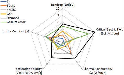
Other important material properties are the critical electric field, which is the maximum electric field in which the material can operate without breakdown, the thermal conductivity, and the saturation velocity of carriers.
By using materials with a higher critical electric field, the operating voltage can be increased, with higher saturation velocity the switching speed can be increased, and with higher thermal conductivity the cooling requirements are reduced. Therefore, systems and powertrains making use of such silicon alternative devices can be more efficient, simpler, more compact and significantly lighter. The figure above compares these characteristics between different semiconductor materials, namely silicon (Si), 3C- and 4H-silicon carbide (SiC), gallium nitride (GaN), diamond and gallium oxide.
Silicon carbide
Silicon carbide is an IV-IV compound material composed of silicon and carbon atoms. It has been produced since 1892 and was used initially for industrial applications for cutting, grinding and polishing.
Due to the chemical bonding between silicon and carbon atoms, SiC exhibits wide bandgap energy and became a promising material for power electronic applications. It can be found in more than 200 crystalline structures, named polytypes. Among all of them, 4H-SiC and 3C-SiC are the most prominent polytypes for power electronic applications, and various semiconductor devices have been demonstrated since the 1990s. 4H-SiC is the only polytype with devices currently available commercially.
Although various polytypes have significant differing crystal properties, SiC in general has a high critical electric field strength, high saturation drift velocity and high thermal conductivity. Therefore, when high-power SiC devices are used in aircraft applications, they can offer improvements in efficiency, power density and reliability. Additionally, for high-altitude applications, like aerospace, radiation immunity is of great importance. Compared to bulky silicon-based converters, SiC ones are more immune to cosmic radiation due to their higher displacement current and lower volume.
However, there are a few reasons why SiC devices have not yet been used widely in high-power applications. Firstly, the device and fabrication process is not mature enough, and secondly, the manufacturing cost is higher than silicon. Additionally, there are still reliability concerns due to defects and traps in the bulk and the interface between the oxide with the semiconductor.
3C-SiC, compared to 4H-SiC, has the potential to give devices with more reliable SiC/SiO2 metal oxide semiconductor (MOS) systems. Also, 3C-SiC bipolar power devices, namely bipolar junction transistors (BJTs), P-i-N diodes and insulated-gate bipolar transistors, can achieve unmatched low loss performance up to at least 5kV [72], making it ideal for aerospace high-power electrical systems and applications. However there are significant technological issues which need to be resolved prior any commercial devices become available.
Furthermore, SiC device packaging is challenging and that originally developed for silicon devices puts limitations on the achievable performance and safe operating area. Finally, high-speed SiC devices produce increased electromagnetic interference during switching transients which can cause a malfunction in adjacent systems.
Another point of concern is the degrading performance of SiC devices at cold and cryogenic conditions. Specifically, the on-resistance increases dramatically and the breakdown voltage decreases as the temperature drops. It is therfore important to carefully design the thermal management system of such power electronics to maintain their performance and controllability within a desired window.
Gallium nitride
Gallium nitride is an alternative wide bandgap semiconductor material that closely competes with SiC, both in terms of performance and technological maturity.
It is currently commonly used in radio frequency applications and light-emitting diodes, and more recently it has started being used in commercial power electronic applications.
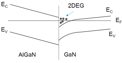
One of the main advantages of GaN is the formation of a quantum well in the heterointerface between GaN and aluminium gallium nitride where a large concentration of free electrons are attracted. This electron channel is called two-dimensional electron gas (2DEG) and significantly increases the deviceʼs conductivity.
Another advantage of GaN devices is the ability to be fabricated using cheap silicon substrates. Throughout almost 30 years of development, various device structures and transistors, have been demonstrated by various manufacturers and research centres revealing the potential of GaN-based devices. However, the material growth and fabrication technology are not mature enough and, as a result, there is a plurality of traps causing reliability issues. Current collapse, dynamic on-resistance and threshold voltage instability are some of them.
Additionally, due to the non-optimised material growth processes and the high trap concentration, fabrication of thick epitaxial layers with low defects density is difficult, restricting the fabrication to mainly lateral devices. The maximum achievable breakdown voltages of GaN devices is therefore rather low for use in high-power aerospace applications. However, GaN is superior to SiC at low-temperature conditions. Specifically, GaN high-electron-mobility transistor devices show improved on-resistance and switching speed, whereas their breakdown voltage is stable.
Beyond the performance of wide bandgap power semiconductors
Apart from SiC and GaN materials, there are other materials with even wider bandgap known as ultra-wide bandgap materials (UWBG). Among them, diamond and gallium oxide are seen as good alternative materials for very high-power electronic applications. These materials offer further theoretical improvements in terms of efficiency and miniaturisation.
Gallium oxide can be found in various crystalline forms like SiC. β-Ga2O3 is a stable structure for a wide temperature range. It has four to five times higher critical electric field than silicon, and native β-Ga2O3 can be fabricated with simple,
low-cost, melt-growth technologies. However, its greatest challenge is poor thermal conductivity, which means heat extraction from a potential device is difficult. When used at lower temperatures though, this becomes less of an issue.
It has poor hole mobility due to the large hole effective mass, and holes suffer from rapid self-trapping. It has known donors – tin, silicon, germanium – but all possible acceptors for p-type doping have very high activation energy, hence it is inadequate for bipolar devices.
Metallisation is a big issue too, with low resistance ohmic metallisation proven to be very challenging. Finally, it is difficult to identify an adequate dielectric material that will be unreactive during the fabrication process, has high interface quality and low trap/defects density, as well as sufficient band offsets with both conduction and valance band.
Diamond has the best electrical properties among all semiconductors for power studied to date. It has the highest bandgap energy, thermal conductivity, electron and hole mobility, and saturation velocities. It can then provide, in theory, the best performing devices.
Nonetheless, its fabrication technology is at an early research stage and the cost is extremely high. In addition, diamond dopants have high activation energies. The latter is of high significance because without appropriate dopants it is not possible to form functional switching devices.
Cutting edge
Diamond seems to be the material of choice when taking into account only the electrical and thermal characteristics. However, to answer which semiconductor technology is the most promising for future aircraft applications, further parameters need to be assessed. The performance of devices and therefore power electronic convertors is linked with the interplay and interaction of the semiconductor material with potential dopants, insulators and conductors (metals). Diamond is particularly poor in this regard, due to the poor performance of any possible dopant species, thus reducing the potential to form devices based on this material. Additionally, the technical maturity and manufacturability can be a limiting factor.
Gaining that maturity is a long-lasting process, for example, silicon technology has been optimised for more than 50 years for high-voltage silicon devices to approach the current maturity and performance. As a result, diamond and gallium oxide materials are not anticipated to play a crucial role in aerospace electronic applications for at least the next 10-20 years. Instead, SiC and GaN have been the focus of significant research efforts in the last 20 years, and have the most potential to serve well the requirements of aerospace and aircraft electrical power conversion. SiC will likely dominate the higher power/voltage conversion and can the lower voltage.
It is worth mentioning that electric aircrafts require power systems ranging from a few watts – such as cabin lighting power supplies – to several mega watts like the electric propulsion system. Therefore, the silicon usage cannot be completely displaced, but all three materials are expected find their place in this wide range of systems where the scope is to optimise the overall performance and efficiency.
The authors would like to thank the FlyZero team, in particular Dr James Minshull ProfGradIMMM, for their support in the production of the Post-Silicon Power Semiconductors advanced materials position paper.