One layer at a time
Paragraf is seeking to advance graphene-based electronic devices using standard semiconductor processes.
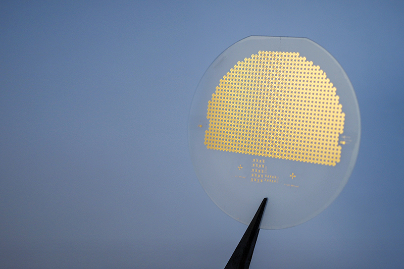
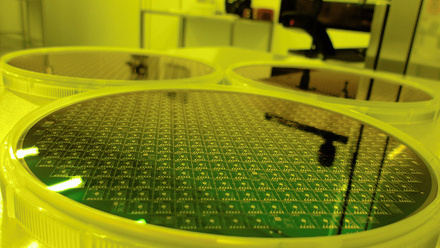
One of Paragraf’s graphene-coated wafers
© ParagrafEntering its fourth year of operation, Paragraf’s 4,000m2 site in Huntingdon, Cambridgeshire, follows in the footsteps of its older site in Somersham, just 14.8km away.
The company is pursuing ambitious plans for expansion and scale-up of its proprietary technology for graphene-based electronics. It specialises in the direct deposition of graphene onto silicon or sapphire substrates via a modified metal organic chemical vapour deposition (MOCVD) process.
The Somersham lab focuses on R&D. 'It’s filled to the brim with equipment that got us to the pilot production stage. It has the capability to take our technology from bare substrate all the way through to finished graphene electronic devices, typically on smaller, two-inch wafers,' says Chief Operating Officer Tony Pearce FIMMM. 'But there’s not enough capacity or capability to do high-volume production. That’s where the Huntingdon building comes in…more than double the footprint.'
The spin-out company stems from research at the University of Cambridge, UK, on deposition processes for gallium nitride and compound semiconductors. Collaborating with a team focused on graphene at the University of Manchester, UK, the group then investigated whether their methods could be integrated with the 2D material.
Pearce highlights, 'There was a great deal of promise for graphene in the electronics industry, but there lacked a manufacturable process.'
Describing the original method for isolating graphene, where layers are peeled off graphite blocks using scotch tape, Pearce says 'that’s not a manufacturing process, but one for scientific discovery. To be useful in electronics, we need to integrate graphene into a wafer-scale process'.
In the mainstream industry, an exfoliation stage involving intermediate copper catalysts 'became the next step for realising graphene on a wafer', but the Paragraf team explains that this presents issues of contamination and quality control. In this process, graphene is deposited onto a copper catalyst, then transferred from that metal layer onto a wafer surface.
Pearce shares, 'Our direct-to-wafer process [instead] uses a modified MOCVD technique traditionally used for compound semiconductor materials like gallium arsenide, gallium nitride and silicon carbide. Our ability to deposit directly on silicon and sapphire – and six-inch wafers – is unique.'
Dr Andy MacInnes, Paragraf’s Chief Development Officer, continues, 'Dr Simon Thomas, our CEO, and Dr Ivor Guiney, one of our Technical Directors, were students of Professor Sir Colin Humphreys FIMMM [at Cambridge]. They developed this modified MOCVD growth technique – the core IP of the company.'
Proving the concept
Paragraf’s early years were spent on the proof-of-concept and getting initial devices in customers’ hands.
Key Account Technical Lead Rosie Baines Warburton has been with the company since October 2018, not long after its inception in 2017. She is a prime example of the small – but growing – team’s commitment to Paragraf’s mission.
Coming into the job straight from her Master’s degree gave her exposure to different project streams. 'We didn’t limit ourselves, looking into lots of different avenues and devices. The main device we were developing back then was the magnetic field sensor.
'From there it grew really suddenly. We got some good early results with collaborators – including testing in partnership with CERN – so there were some nice early wins. We were a small team making devices using limited resources, so it was nice to get that recognition. It helped us gain confidence and grow, and we’ve retained that atmosphere. It’s been a fantastic journey.
'The team continually improved the initial technology to get the quality and scale of its graphene to its current state. They are even branching out to other 2D materials – while graphene’s two-dimensionality makes it a superior conductor, insulating materials can be produced using the same method.
The challenge now is scaling up further. This is achieved partly through increasing wafer size – going from two to six inches gives almost 10x more area and more devices per wafer – but also upgrading from lab- to production-scale equipment.
The devil’s in the detail
To produce graphene, traditional modified MOCVD deposits organic, carbon-containing molecules on copper substrates, where it precipitates as pure carbon. In peeling off the graphene, either mechanically or via electrolysis, contamination can occur from the copper, original precursors, or electrolyte solutions.
To avoid this, Paragraf 'grows films directly onto the electronic substrates', shares MacInnes. 'Whether it’s a two-, six-, or 12-inch wafer, there is a single layer of graphene across that whole wafer. It’s perfectly contiguous, so it doesn’t have holes.' He says the capability to produce six-inch wafers has 'existed all along', even in the old facility. 'We just didn’t have the tools to process them.'
MacInnes calls the graphene 'pseudo-epitaxial', as it has large grains, but says, 'we’ve retained more mobility than we would with multiple transfer methods. All the fast electronic materials we are used to, graphene surpasses them in mobility and electronic properties. It’s also almost its downfall in how you have to handle it'. The free carriers in the layer will interact with any material it encounters.
Paragraf does 'all the standard operations' of a compound semiconductor fabrication plant (fab), but some modification is required to preserve graphene and retain its superior properties. Pearce adds, 'If it becomes multi-layer, it’s not graphene anymore, it’s graphite.'
He explains that the precursor, or source material, is 'highly sensitive, to the point where it’s even restricted within the business. If you’re not directly involved in the graphene deposition, that information is restricted – that’s normal practice'.
However, he shares that the graphene precursors are 'very low risk' compared to the flammable and hazardous gases used in compound semiconductor deposition, such as silane, arsene, or phosphene. He asserts that manufacturing costs are also lower than in the mainstream industry, because there are fewer scrubbing and detox requirements and less precursor material is needed to produce the single-atom-thick layers.
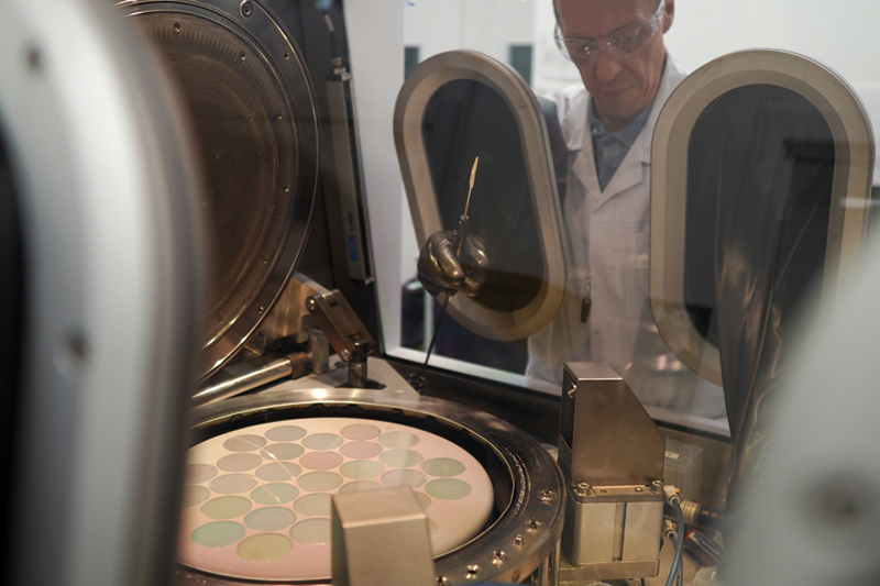
A researcher working on the modified metal organic chemical vapour deposition machine
© ParagrafWhere the magic happens
Putting on white lab coats, clear goggles, shoe covers and gloves in the 'gowning room' for 'an authentic experience', Pearce takes me on a tour of the Huntingdon facilities.
He begins, 'What you’ll see when we walk around is larger-scale, higher-volume equipment, similar to what you’d find in semiconductor fabs, but we’ve focused them and adapted our process for 2D materials.'
We start with where the material deposition happens. The reactor labs in the ‘grey room’ contain both automated machines and manual worktops. The precursor is delivered in gaseous form to the wafer surface, depositing a graphene layer.
The robotics in the deposition machine are not in operation when we view them, but Pearce explains how the parts operate in isolation from each other, useful for when any given element requires maintenance. 'Robots have bad days too, so we keep an eye on it to make sure it’s behaving itself. We can work on one chamber while the others are running.'
A fork mechanism picks up the wafers from a cassette, transferring them through a port into the reactor chamber. Pearce says, 'At the moment, we just have one process module here, with what’s called a cluster tool, but we are able to connect another three.' Although there are gloves attached to the reactor chamber, these 'are really just to keep the area clean, for maintenance, things like that', rather than to perform any processes manually.
A software controls delivery of the proprietary precursor to the reactor chamber, with a shower head-style reactor that distributes gas across the wafer through thousands of tiny holes. During this process, the wafer is rotated to ensure uniform deposition. Processing conditions – temperature, pressure and timings – are all machine-controlled.
'All these front-end robotics are standard. In a large silicon fab, you might see different process modules connected, but the system is generic, so it has very high reliability. And we’ve got lots of optical monitoring tools to measure what’s happening in real time,' reveals Pearce.
One researcher is working manually in the lab as we walk around. Pearce explains, 'This is an evaporation system for metals, so he will be loading a wafer with graphene into a metal deposition process.' He jokes, 'When they know I’m coming in here, everyone disappears – that’s why there’s only one person in here, he couldn’t get away!'
More seriously, 'We are running regular production starts in here. Even though it looks like nothing’s happening, it is – when you’ve been here long enough, you learn to notice what the machine is doing from the sound.'
Another modified MOCVD machine in the next room is 'the first one we got running in Huntingdon'. Pearce says it was 'rescued' from a gallium nitride semiconductor fab and 'repurposed for graphene'.
Installing identical machines at Huntingdon helps recreate and scale Somersham’s R&D-level processes. The exteriors look the same as those in compound semiconductor fabs, but internally they are modified for Paragraf’s six-inch wafer manufacturing process. While the current tools still require manual loading, Pearce shares that, in the coming months, they will be transferring from these older systems to 'state-of-the-art', fully automated machines.
'We’ve jumped very quickly to standard production tooling for compatibility with the rest of the industry. It’s important the systems can be integrated into the mainstream semiconductor industry with as little bespoke, special magic as possible.'
Keeping it clean
We peek through a window into a small passage that connects the grey room to the orange-yellow etch cleanroom, coloured this way to preserve photosensitive materials for photolithography to pattern the wafers’ surfaces. 'This is the cleanest room in the building,' Pearce says.
He explains that a machine passes wafers through a hatch from the grey room, and another robot in the cleanroom picks them up. 'We don’t put people through that.' Those working in the cleanroom must gear up in a full suit, hood and face mask, then pass through an air shower to maintain ultra-cleanliness.
The cleanroom also houses equipment for device layouts and metrology to check the wafers’ dimensions. Pearce continues, 'We don’t have robot tracks, so there are people involved in moving the cassettes from one tool to another, but once they’ve been delivered, the robots within each one will take over.
'In high-volume fabs, you see overhead robots travelling around with 12-inch wafers, but for our six-inch manufacturing process, that’s not necessary.'
Once etched, contacts are added to the graphene patches based on the end device’s design (front-end-of-line). The wafers are diced up into individual devices, tested and packaged (back-end-of-line). The dicing step currently occurs offsite.
When we view the cleanroom again from the expansion room, I comment that it’s hard to look at continuously. Pearce laughs, 'Yes, when you come out again after working in the yellow room for a long time, everything looks a different colour!'
Future spaces
The vast expansion room, which currently lies half empty, feels laden with potential. Pearce says, 'This was originally an empty warehouse-style building, so we put our own clean facilities in, which involves not just investment in the latest equipment, but also the rooms themselves – gas pipework, water, gas and electricity delivery. Everything has been done from scratch.
'It’s all either delivering clean, filtered, temperature-controlled air for the cleanrooms, process cooling water, gas supplies, or extracting air away. A great deal of investment, time and thought process goes into the facility’s design, as into the technology itself. It’s almost as if the smaller the material gets, the bigger everything around it has to be – all focused on producing one atomic layer of carbon.'
A new workspace module is being installed as we speak, with people walking around in high-vis jackets. This will eventually house wet process machines – chemical workstations for etching and cleaning wafers. The wet benches will again be nearly identical to those in a typical semiconductor fab.
Roughly 50% of the building’s footprint has been filled so far, but Paragraf is planning to fill it completely, mainly installing more cleanrooms to satisfy forecasted demand.
Pearce emphasises that Paragraf is generating its own demand and market, so although they’re ambitious, they cannot know exactly what the rate of adoption will be and how their technology will evolve. 'I can almost guarantee we’ll want this factory to be different in three or five years’ time.'
Building out modularly, in phases, allows for more funding to come in and greater design flexibility. This is crucial when 'creating products that don’t exist anywhere else in the market'. On completing the tour of what Pearce calls 'phase one' of the expansion, he adds, 'we’re already making plans for the subsequent phases'.
Paragraf’s aim is to compete commercially with other semiconductor devices on the market. Their rapid scale-up is two-fold, combining an increase in the production capacity of individual machines with a greater number of machines.
Pearce’s role in operations is largely focused on preparing the infrastructure for future production. It takes months to over a year of planning, with long lead times on equipment. But Paragraf also has an advantage, as their carbon-based, organic precursor supply chain is simpler and doesn’t rely on critical minerals as much as the mainstream industry.
Additional capacity will come from producing higher volumes with the deposition tools already in operation, as well as other steps like processing. Each larger wafer produced could generate hundreds or thousands more devices, so 'increasing capacity in areas like photolithography' will avoid creating manufacturing bottlenecks.
Most of Paragraf’s funding comes from venture capital rounds. It has just finished Series C, which Pearce says contributed to much of the Huntingdon construction. 'We’ll be doing that again to fund our next phase of expansion.' Innovate UK also funded a few specific products.
Automation and artificial intelligence (AI) are starting to play a part in development. More repeatable, uniform and cleaner material deposition is better for mass production, enabling increased yield and output. Pearce also notes an acceleration in more sophisticated tools for analysing data from testing and manufacturing, in place of manual quality control processes.
'I used to spend hundreds of hours looking down a microscope at failure modes of devices. We’re now developing our own capability to run self-learning of optical inspection – to identify defects and issues that are harder to spot by eye. This makes sure testing gets better, not worse.'
Paragraf has had to develop its own testing process because 'traditional metrology and measurement techniques don’t work for 2D materials'.
A multi-functional solution
Everyone I speak to at the site emphasises graphene’s versatility. Baines Warburton says, 'even when you zoom into one application, like molecular sensing, it’s still this blank canvas you can functionalise in many different ways. That’s almost one of graphene’s pitfalls, that indecisiveness of what to pursue. You could be frozen on the spot, not knowing which avenue to go down. If a customer says, ‘Can you detect this?’, I can never say no straight away, because it can always be explored.'
An exemplar application is the graphene field-effect transistor, or GFET. MacInnes explains that these are 'incredibly sensitive current detectors that exploit a unique feature of graphene conductivity called the ‘Dirac point’ to quantify and track the merest of potential changes occurring on an exposed surface of this single-atomic-layer material.
'These were initially aimed at the electric vehicle market, to detect anomalies and identify failures early on in individual cells of battery packs'.
Despite being simple structures, graphene on the GFETs can detect a molecule hitting its surface. 'They can detect a whole alphabet soup of chemicals and molecules. We produce a basic vehicle that a receptor layer can be added onto for customised detection,' says MacInnes. The GFETs can detect viruses, bacteria and even single molecules, offering a 'vast array of applications'.
The company is preparing to produce large volumes of these for other businesses to functionalise themselves. MacInnes continues, 'We’ll do the foundry, they can do their business products.' The basic GFET unit is a multi-channel device – a plug-in board – and Paragraf gives notes in a white paper to potential customers on how to functionalise and read results from their GFETs.
Meanwhile, MacInnes says the GFET discovery kit is a 'plug-and-play – it’s got the same detective sensor, but also black box electronics, where it will display readouts of interest – everything’s interconnected'.
Customers can add their sample, functionalise it, then get readouts in standard formats compatible with most software platforms. This ease of discovery can help 'universities and other small operations get on the discovery platform very quickly', where other, larger companies might already have that capability internally.
Medical diagnostics is a prime area for GFETs. If they were available during the COVID-19 pandemic, MacInnes claims they could have been functionalised for diagnostics.
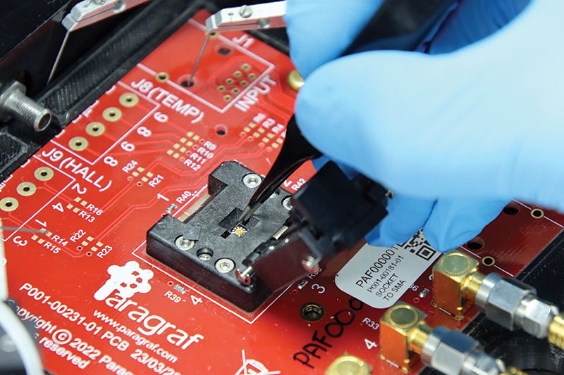
Scaling up includes increasing the capacity to manufacture devices from the graphene wafers that Paragraf produces
© ParagrafTrade secrets
Many of Paragraf’s developments are heavily under wraps, but everyone seems excited for the future. They are currently exploring other 2D materials and the possibility of producing multi-layer heterostructures, which Pearce says, 'unlocks a whole different capability for future electronics'.
MacInnes highlights 'hexagonal boron nitride (hBN) and a class of compounds called transition metal dichalcogenides (TMDs)', of which molybdenum disulfide and tungsten disulfide 'are probably the most studied'. Structure-wise, these 2D materials are 'analogous to graphene', but with different symmetry and properties. The semi-metal hBN is a wide-bandgap insulator, while TMDs are semiconducting. These Van der Waals material 'building blocks' can be bandgap engineered to interact with each other in particular ways and produce desirable properties.
'Our demonstration vehicles are building the portfolio of how to handle and harness the properties of each of these materials,' explains MacInnes. He believes combinations of these could help solve heat leakage issues in complementary metal-oxide-semiconductor (CMOS) devices and AI chips, while retaining computational speed.
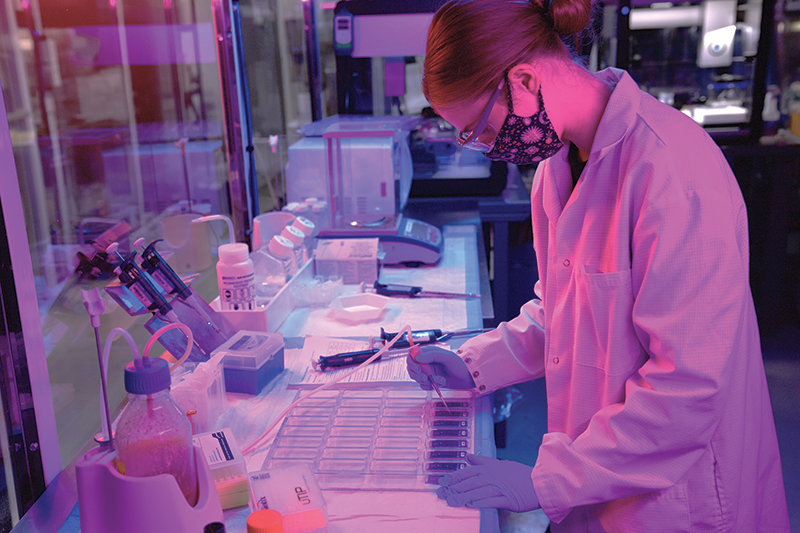
There is still hands-on work in the labs at Huntingdon, but this is more focused on specific areas of the manufacturing process
© ParagrafIn it for the long haul
One thing they can talk about is growth outside the UK. This includes a San Diego office in the US, which came with their acquisition of biocompatible graphene semiconductor company Cardea Bio. There are also new sales and support offices in Abu Dhabi in the United Arab Emirates, and in Shanghai, China, with tentative plans to open a manufacturing facility in Abu Dhabi.
When Baines Warburton started at Somersham in 2018, she says they had 'two or three labs, which didn’t have much equipment, and five of us in the tech team – one or two making graphene, then the others making devices and doing characterisation. That was nice, because I got to do lots of device and graphene characterisation, and learn lots of different process work. It was very manual and hands-on, like depositing contacts onto devices – we didn’t have proper deposition systems. It was mechanical and immediate'.
In the earlier years, 'you’d be trained on everything', whereas people joining Paragraf now tend to be more focused. Employees can undergo 'proper' training on specific equipment, but it must now be requested, logged and approved.
She continues, 'I’ve now moved to the commercial team. There’s a production team to do the processing and process development experts. A lot of us who used to be hands-on are now managing teams.'
She still gets to use her technical background in discussions with customers and clients, but it has brought a whole new set of skills too, including use of customer relationship management systems, quoting, discounts and negotiation processes; as well as designing and scoping out custom projects.
She highlights working with CERN and other big names in the industry, as well as being in the top three nominees for the Royal Academy of Engineering’s MacRobert Award in 2023, as 'proud moments'.
A lot of people in the company are 'personally invested, just from the way we treat each other'. Baines Warburton says celebrations of milestones like work anniversaries feel like 'almost a daily occurrence sometimes…with cake everywhere. Things like that are a really good sign'. At one point during our interview, CEO Dr Simon Thomas pokes his head into the room to say hello, exemplifying Paragraf’s close-knit nature.
She continues, 'I can see how much [the firm] changed. I would never have envisaged what it looks like now, partly because I didn’t know what that should look like. And there might be more to come that I have no idea about – that’s really exciting!'
Pearce has done a fair number of site tours with customers and partners recently, to showcase Paragraf’s achievements and raise the profile of 2D materials. The team is communicating their position – and the UK’s – in 2D materials as much as possible, 'because it’s not all about silicon, or design of the latest graphics processing units and compound semiconductors'.
'What we’re doing here is bringing those 2D materials to market first, ahead of anybody else. We’re using new and advanced materials to keep up with the insatiable power and performance demands of modern electronics.'