Laser-based method unlocks nanofabrication
A method for interfacial imprinting of ultra-thin nanowires could advance wireless, electronic devices, including for wearable or implantable healthcare monitoring.
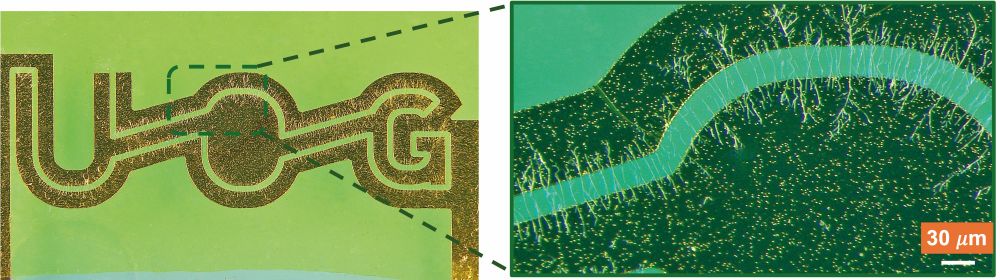
Researchers at the University of Glasgow, UK, share how ‘interfacial-dielectrophoresis (i-DEP)’ allows for precise patterns with 'full degrees of freedom' in nanowire alignment on flexible polymer substrates. This can be achieved without transfer steps.
Combined with a laser post-treatment, the technique is said to overcome the long trade-off between conductivity and transparency, simultaneously. The resulting films reportedly demonstrate superior transparent and highly conductive electromagnetic interference (EMI) shielding.
Nanowires have potential for high-performance flexible electronics, but existing methods lack programmable and deterministic alignment, says Research Associate Jungang ‘Judy’ Zhang. This limits reliable integration onto flexible substrates and creates challenges for manufacturing efficiency, scaleability and consistent device performance.
In this work, silver nanowires are first aligned on a thin, flexible, transparent polyimide film using a non-uniform electric field. Controlled electric field gradients generated by strategically designed microelectrodes manipulate the nanowires’ positions and rotations across large areas.
This is followed by non-contact welding of the nanowire junctions through exposure to ultra-fast, picosecond pulses of laser light. This enables electrical interconnections and strips the nanowires’ coating of insulating material, increasing optical transparency by up to 10% and reducing electrical resistance by a factor of 46.
Professor Hadi Heidari from the university says, 'The EMI shielding performance of the materials we created…improves on the performance of non-aligned nanowires by more than a thousand times.'
Prototype 5.1µm-thick films made by i-DEP reportedly achieve over 35dB of shielding effectiveness across frequencies of 2.2-6GHz, blocking more than 99.97% of electromagnetic radiation, while maintaining 83% optical transparency.
Structural nanogaps in the network are key to the interference resistance. The gaps act as capacitors that reduce the effects of external signals such as 5G and Wi-Fi on internal electronics, useful for sensitive equipment like medical devices. The researchers call this a ‘capacitively-coupled interwire network’.
Zhang adds, 'Notably, this represents one of the first demonstrations of local, substrate-specific, nanostructure alignment using i-DEP, combined with a laser post-treatment that enhances both optical and electrical performance.
'For flexible displays, wearable devices and implantable medical technologies, this shielding capability, paired with a high degree of transparency, is crucial. It ensures high-purity signal transfer for real-time healthcare monitoring while blocking unwanted electromagnetic noise.'
Conventional cleanroom fabrication is often limited to small wafer sizes and requires expensive, time-consuming processes, but i-DEP is reportedly capable of larger-area fabrication without cleanroom facilities or transfer steps.
Demonstrator 40x80cm devices have been created, and the researchers claim the technology can be scaled up for manufacture, with reusable electrodes and high-speed laser microfabrication.
The technique can also be applied to a range of metallic and semiconductor nanowire and polymer materials with variation in the applied AC electric field.
Zhang says their next steps for commercialisation include integrating i-DEP into large-scale, roll-to-roll manufacturing and partnering with electronics developers in various applications.
They are looking to combine the i-DEP alignment method with sensing, energy harvesting or integrated circuitry, as well as applying it to biocompatible and wearable devices.