Edging closer to 2D control
A new technique to control the edges of 2D materials offers research opportunities
‘Our method makes it possible to control the edges [of 2D materials] – atom-by-atom – in a way that is both easy and scalable, using only mild heating together with abundant, environmentally friendly chemicals, such as hydrogen peroxide,’ says Battulga Munkhbat, a Postdoctoral Researcher in the Department of Physics at Chalmers University of Technology, Sweden.
He outlines how manipulating the edges of 2D materials has previously been a challenge as they are very different to the main body of the material. Transition metal dichalcogenides (TMDs), for example, have a specific type of edge with magnetic and catalytic properties.
Typically, TMDs have two different variants of edges – zigzag or armchair. Calculations predict that zigzag edges are metallic and ferromagnetic, whereas armchair edges are semiconducting and non-magnetic. Similar to those variations in physical properties, it has been theorised that the chemical properties of zigzag and armchair edges are also very different. Attempting to change the properties using a chemical, the team found that hydrogen peroxide dissolves armchair edges, while leaving zigzag ones unaffected.
The hydrogen peroxide was applied through an anisotropic wet etching process, combined with standard top-down lithographic methods, creating perfect edges.
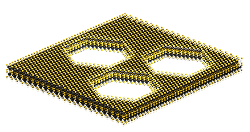
‘It was not only that one type of edge was dominant over the others, but also that the resulting edges were extremely sharp – nearly atomically sharp,’ says Munkhbat. ‘This indicates that the “magic” chemical operates in a so-called self-limiting manner, removing unwanted material atom-by-atom, eventually resulting in edges at the atomically sharp limit. ‘The resulting patterns followed the crystallographic orientation of the original TMD material, producing beautiful, atomically sharp hexagonal nanostructures.’
‘This method opens up new and unprecedented possibilities for van der Waals materials (layered 2D materials). We can now combine edge physics with 2D physics in one single material. It is an extremely fascinating development,’ adds Associate Professor at the University, Timur Shegai.
Shegai notes that following the wet etching process, a flake of 2D material is exfoliated and nanopatterned by conventional lithography – such as electron beam lithography or similar – which results in formation of perfect edges. ‘The complexity of the resulting pattern is predefined by the lithography step.’
The team plans to explore potential applications of the edges, ranging from quantum electronics to new types of nano-devices, and then commercialise their ideas. To this end, they have founded a start-up company offering atomically sharp TMD materials.